4 Experimental Procedure
Required Tools:
- Analog Discovery 2 Board (AD2)
- Soldering Iron
Required Components:
- 16ZLH680MEFC10X12.5 (electrolytic \(16~V\) \(680\mu F\))
- A758EK107M1CAAE018 (polymer electrolytic \(16~V\) \(100\mu F\))
- CL31A106MAHNNNE (ceramic X5R \(25~V\) \(10\mu F\))
- TL431AFDT,215 (TL431 shunt regulator IC)
- Assorted 0603 resistors & capacitors
- Blank FR-4 board and copper foil tape
4.1 Lab Setup
This lab uses the Analog Discovery 2 board and the Digilent WaveForms software. The WaveForms software is supported on Windows, Linux, and OSX and can be downloaded here.
For data analysis and modeling transfer functions this lab and following labs use Python3 and the Python3 matplotlib, NumPy, Pandas, SciPy, and Control libraries.
These python packages can all be installed via the python pip or Conda package managers. If freshly installing Python3 the Anaconda install may be the fastest way of getting started.
For either the Python package managers the names of the packages to install are:
  matplotlib
  numpy
  pandas
  scipy
  control
You will be running two Python scripts. The first, tf_fit.py, will be used to extract a best fit transfer function from measured data. The second, system_tf.py, will be used to model the system you are characterizing. Download links for the scripts are below:
4.2 Measuring Components
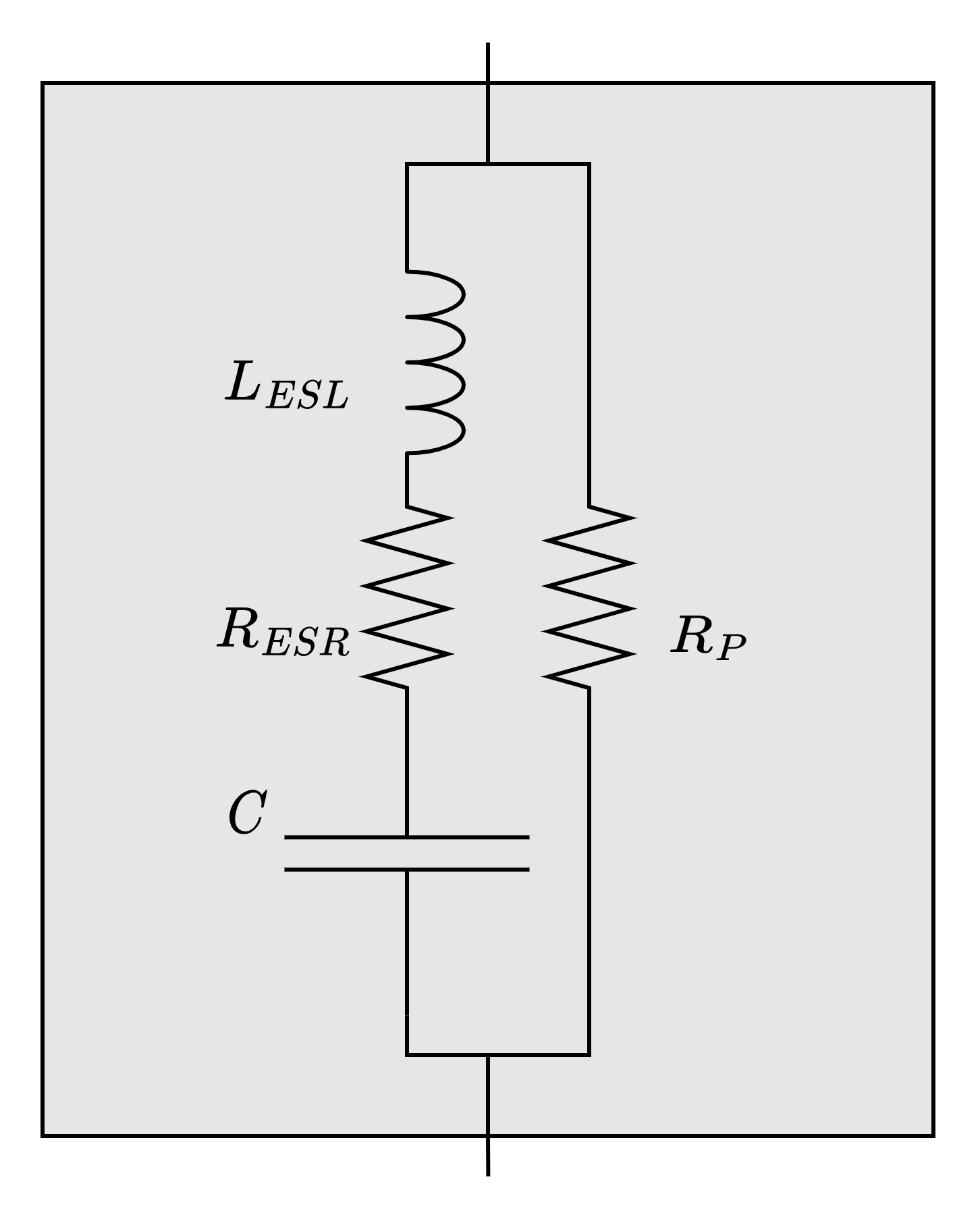
Electrical components are not ideal and sometimes these non-idealities lead to significant disparities between simulated and measured behavior. Understanding these non-idealities is often important in circuit design, especially so in power electronics. Figure 4.1 shows the capacitor model with all of the typically considered parasitic circuit elements. \(R_{ESR}\) is the equivalent series resistance (ESR), \(L_{ESL}\) is the equivalent series inductance (ESL), \(C\) is the nominal capacitance, and \(R_P\) modeled capacitor leakage. Capacitor ESR is determined by the electrode resistance and dielectric loss of the capacitor. ESL represents the inductance of the capacitor electrodes and leads and is largely determined by the geometry of the capacitor. In power electronics the ESR and ESL of the capacitor are typically the most relevant. Both ESR and ESL reduce the ability of the capacitor to filter transients and ESR drives \(I^2R\) loss that reduces efficiency and can lead to the capacitor over-heating.
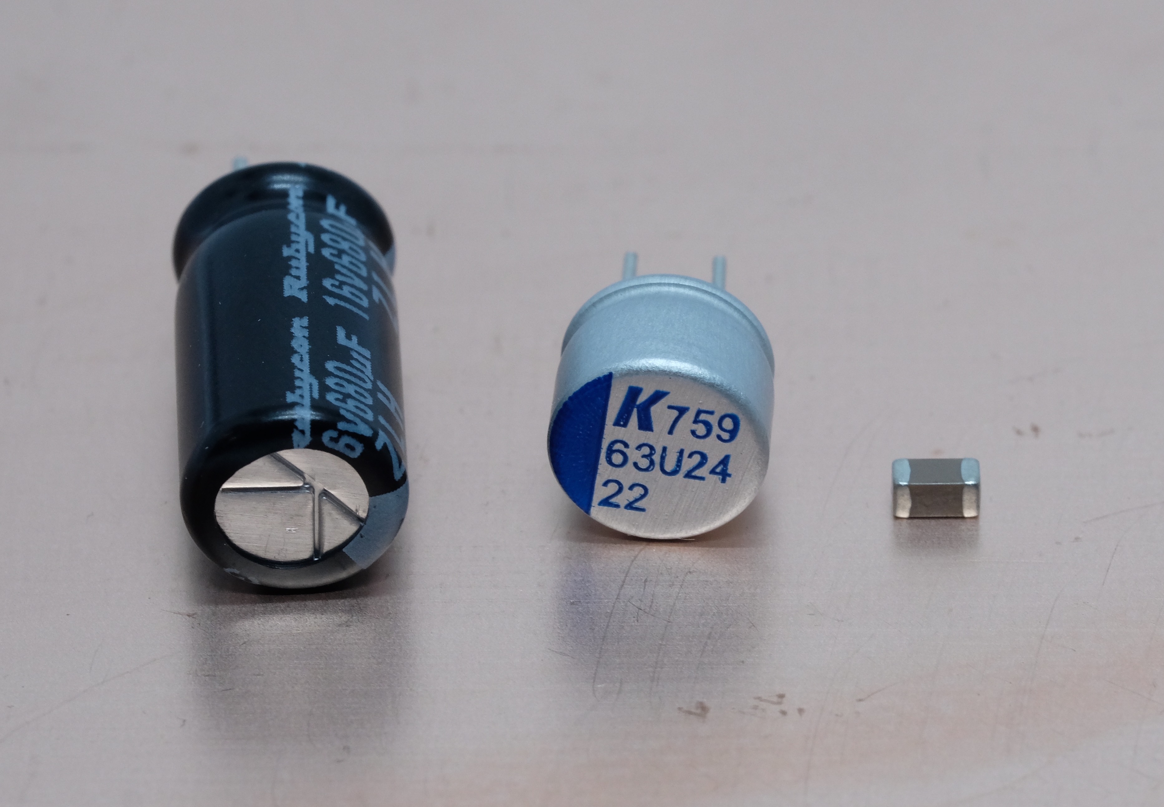
Different capacitor technologies lead to capacitors with varied optimizations for ESR, capacitance, and size. Understanding these differences is important in creating effective designs. In this portion of the lab you will be using the Analog Discovery 2 (AD2) to take frequency domain measurements of the capacitance and ESR of three common types of capacitors: electrolytic, polymer electrolytic, and ceramic. After taking your measurements you are going to be doing some basic calculations to better understand the trade-offs between each capacitor type. Generally, electrolytic capacitors are high capacitance and inexpensive but have a high ESR, polymer electrolytic capacitors have a lower ESR but typically have a lower capacitance and are more expensive, and ceramic capacitors have the lowest ESR and smallest size but are not produced in large capacitance values and are the most expensive for a given amount of energy storage. Both electrolytic and polymer electrolytic capacitors also have a finite life due to the evaporation of the electrolyte they contain. In Figure 4.2 we provide a photo of examples of these three capacitor types.
4.2.1 Measurement Setup
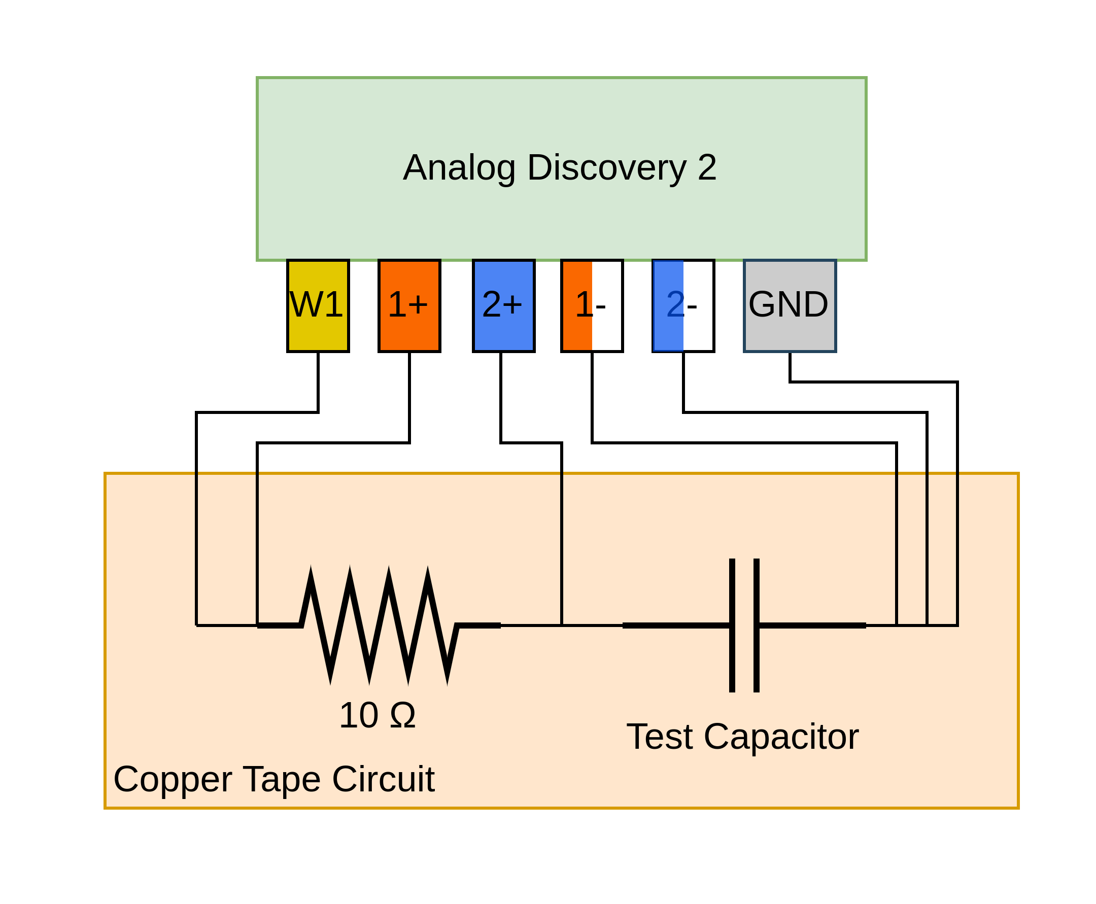
For these measurements you are going to be using the impedance analyzer portion of the WaveForms software. Measurements are made by connecting a known value resistor in series with the capacitor, creating a voltage divider, and applying a frequency sweep with the Analog Discovery 2 (AD2) waveform generator. The oscilloscope channels of the AD2 are used to measure the amplitude and phase of the voltage and the impedance is derived from the reference of the known resistor value. You are going to be soldering the resistor, capacitors to be tested, and wire loops for the AD2 test clips, as a copper tape circuit. Figure 4.3 shows the diagram of the circuit along with the color coded AD2 test leads. In taking your measurements try to connect the test leads for channel 2 as close to either side of the capacitor as possible, as any leads or copper tape between the capacitor and the test leads will contribute to the measured ESR. As the applied voltage is low you do not need to worry about the polarity of the electrolytic capacitors.
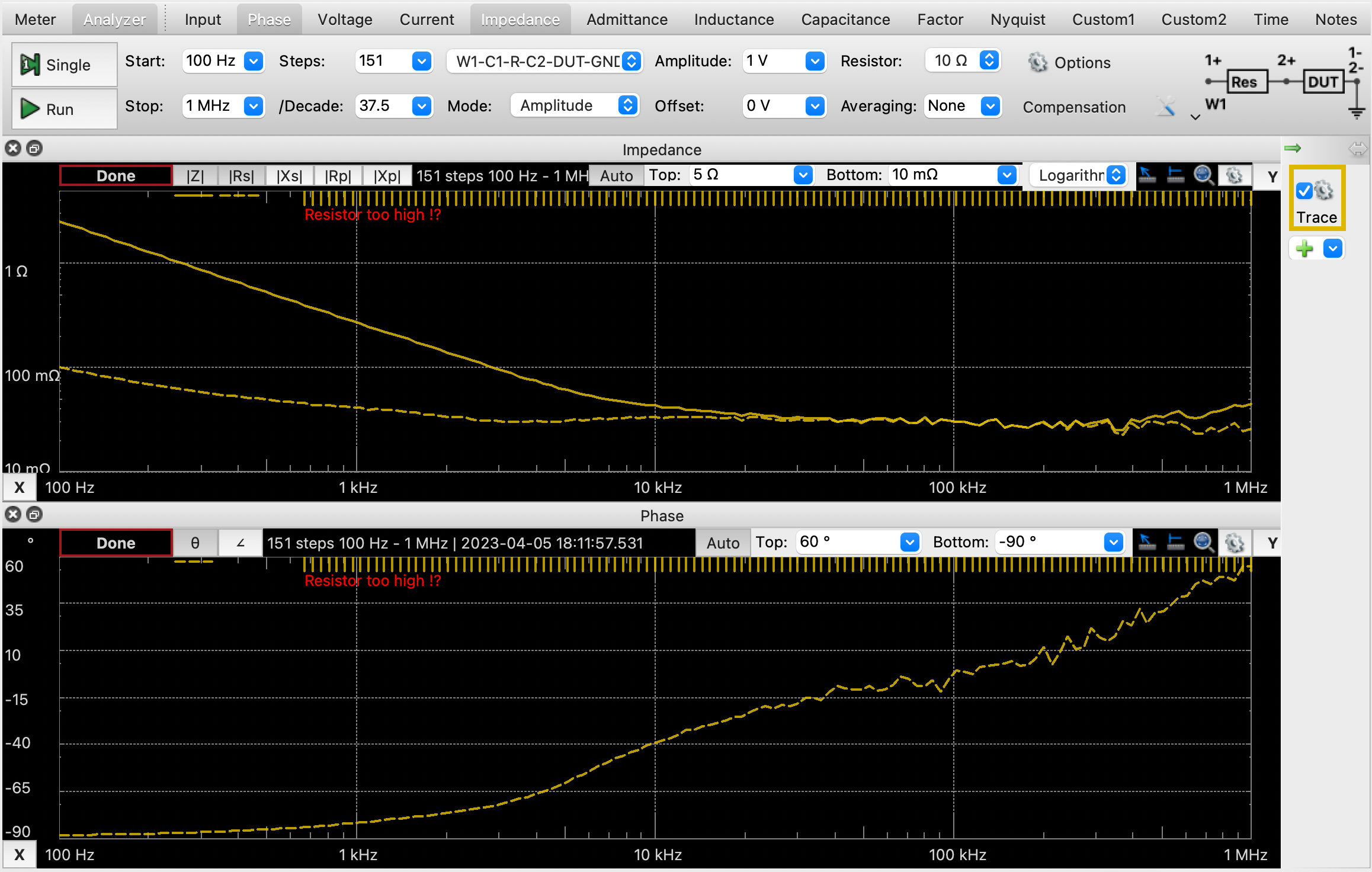
For settings in the impedance analyzer view of the WaveForms software make sure that the measurement mode is “W1-C1-R-C2-DUT-GND”. Use a frequency range of 100 Hz - 1 MHz and an amplitude of 1V. Figure 4.4 shows a screenshot of the settings and example data. A warning of “Resistor too high !?” is to be expected and is due to the low values of ESR being measured. If the channel 2 test clips are connected close on either side of the capacitor the measurements should still be accurate.
4.2.2 Measurement Analysis
The WaveForms Impedance analysis tool measures the complex impedance (amplitude and phase) of the capacitor as a function of frequency. In Figure 4.4 the impedance of the capacitor is shown in the top graph as a solid line and the resistive component of the impedance is shown as a dashed line. Phase is shown in the bottom plot as a dashed line. The capacitor impedance is best interpreted in the context of the Laplace domain. The impedance of a capacitor with ESR can be modeled as a one pole, one zero, system. This is expressed as:
\[ Z(s) = \frac{1+s C R_{ESR}}{sC} \]
At frequencies above the ESR zero at \(\omega = \frac{1}{C R_{ESR}}\) the resistance of the ESR dominates and the measured capacitor impedance is largely resistive. Below this frequency the impedance is largely capacitive. If the capacitor has long leads the added inductance may introduce a second zero causing the impedance to rise at the high frequency end of the sweep.
The capacitance of the tested capacitor can be calculated from the measured impedance at any frequency substantially below the ESR zero where phase is close to \(-90^{\circ}\). The value of \(R_{ESR}\) can be taken from any frequency where phase is close to \(0^{\circ}\) and the impact on the capacitance value is minimal. Use the “Quick Measure” tools on the upper right corner of each plot to aid you in reading off values. Due to its low ESR value the ceramic capacitor phase may never change. If so, approximate ESR based on the lowest value from the \(R_s\) line on the plot.
You may notice that the displayed value of \(R_s\) at low frequencies is significantly above the \(R_{ESR}\) value you are measuring, which is not predicted by the one pole, one zero model. This is due to dielectric loss in the capacitor which manifests as a (typically slight) deviance from the expected \(-90^{\circ}\) phase angle of a capacitor and a series resistance proportional to the capacitance impedance. The ESR value relevant to the ESR zero and measured in this lab is determined by the electrode resistance of the capacitor. When used for output filtering the capacitor voltage ripple is typically small and the switching frequency is often above that of the ESR zero, so the high frequency ESR determined by electrode resistance dominates any losses due to dielectric loss.
By convention transfer functions use angular frequency, which is referred to with variable \(\omega\).
For conversion, \(\omega = 2 \pi f\)
4.2.3 Tasks
- Using the AD2 measure the capacitance and ESR of three capacitors: 16ZLH680MEFC10X12.5 (electrolytic) A758EK107M1CAAE018 (polymer electrolytic), CL31A106MAHNNNE (ceramic)
- (Post Lab) You are considering using the capacitors for output filtering of a boost converter with a 50% duty cycle and a 0.5A output current. Assume the inductor has negligible ripple. Based on your measured values for ESR and capacitance, which capacitor would provide the lowest voltage ripple at 10KHz? At 2MHz?
- (Post Lab) You need to select one of the capacitors for filtering the 120Hz ripple from a rectified AC transformer. Assuming you could use multiple of the (more costly) ceramic or polymer electrolytic capacitors to match the capacitance of the electrolytic capacitor, would the lower ESR of either of the capacitors lead to a significant reduction in ripple?
4.3 Capacitor Networks
In this part of the lab you are going to see how more is not always better. Specifically, how adding more capacitors can actually provide worse filtering at some frequencies. When different capacitors are connected in parallel there can be a resonance between the ESL and trace inductance of one and the capacitance of another. This situation can arise when electrolytic capacitors with a large ESL or long connecting traces are connected in parallel with a smaller ceramic or film capacitor. Around resonance the impedance of the parallel capacitor network can be significantly greater than the impedance of either capacitor in isolation. Additionally, a parallel resonant network sustains a circulating current higher than the input current. If a harmonic of the operating frequency of a SMPS falls close to a parallel resonance in the filtering capacitor network the ripple attenuation may be worse than expected and the capacitors may be exposed to unexpectedly large ripple currents.
4.3.1 Tasks
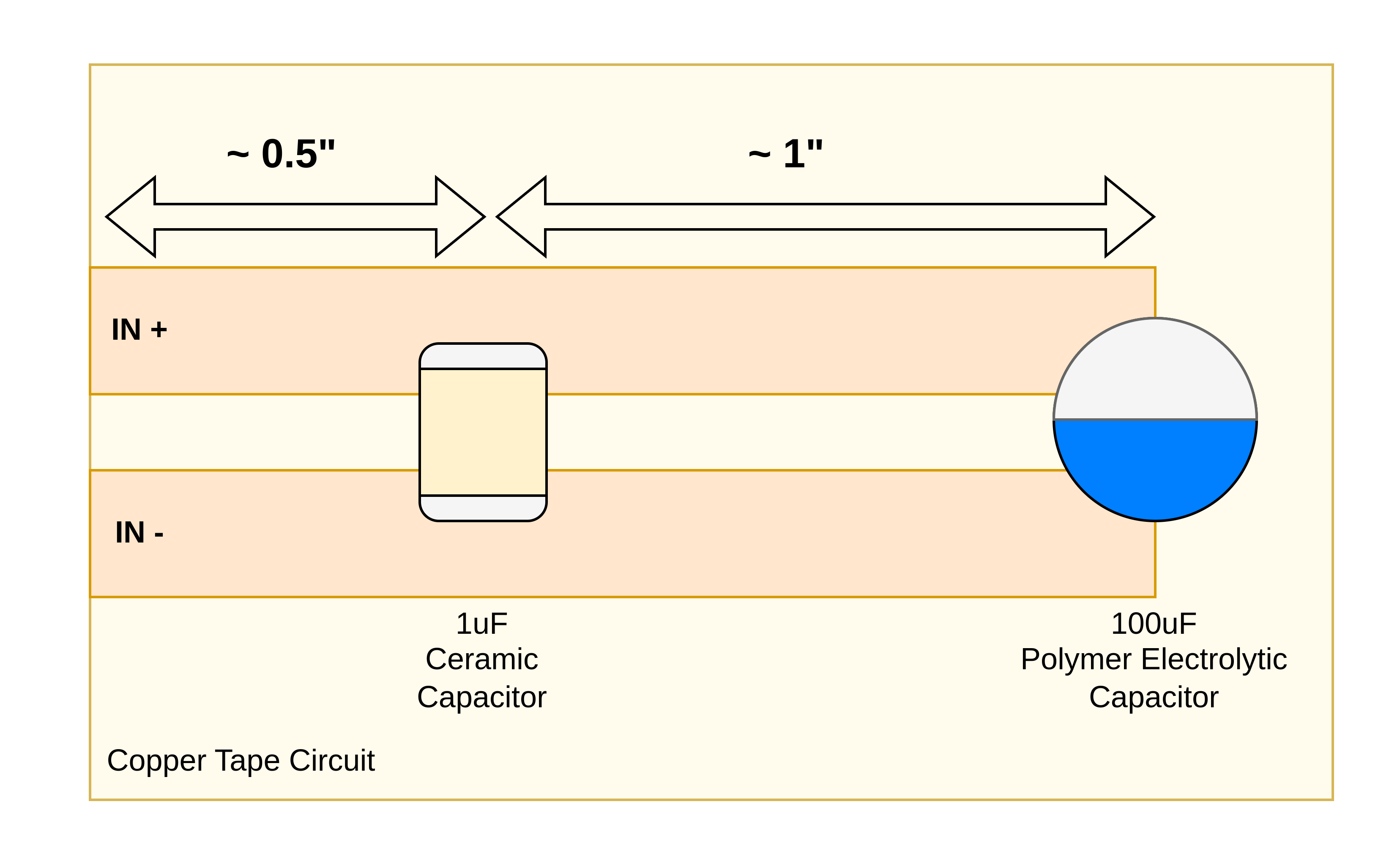
- Draw the equivalent circuit diagram of the circuit shown in Figure 4.5, including the inductance of the copper tape traces and capacitor ESL.
- Construct the copper tape circuit shown in Figure 4.5. Any package size SMD ceramic capacitor can be used. For the polymer electrolytic capacitor use the part you used for the first part of the lab. Measure the impedance of the network with the AD2 from 1kHz to 10MHz and save the plot.
- From the measured impedance curve and resonant frequencies of your circuit calculate the values of the inductances in your equivalent circuit diagram.
- At what frequency does the capacitor network have the highest impedance compared to either capacitor in isolation? How many times higher is the impedance?
- What circuit values could you change to reduce the maximum impedance of the parallel resonant peak?
4.4 System Transfer Functions and Loop Stability
In this part of the lab you are going to be measuring the open loop frequency response of a system and observing how it can be used to predict the stability of the system when feedback is used for regulation. These measurements are going to be taken on a simple linear regulator circuit using the TL431. This system has fewer components and failure modes than the flyback test board you will once again be working with in the next lab, but the same core principles apply.
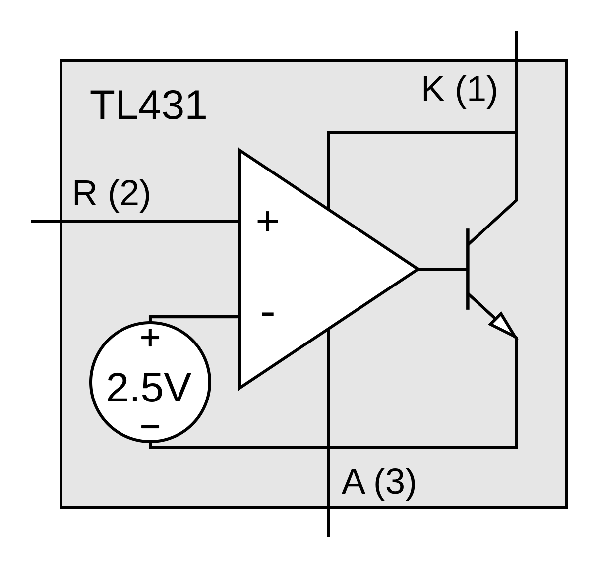
Datasheets for the TL431 typically call the device a shunt regulator, but is an incredibly versatile and widely used IC that only costs a few cents in volume. Just a few of the possible uses of the TL431 are as a linear regulator, comparator, amplifier, or voltage reference. In one of the largest commercial uses the TL431 is used for regulation on the secondary side of isolated switch-mode power supplies to drive an opto-coupler that controls the power stage on the primary side. A diagram of the internal circuitry of the TL431 is shown in Figure 4.6. The TL431 is a three terminal device containing an op-amp and voltage reference and is powered through the output (cathode) pin. The reference terminal (R) is connected to the positive input of the internal op-amp and the internal 2.5V reference is connected to the negative input of the op-amp. The op-amp drives the base of an internal NPN transistor which is used to sink current from the cathode pin (K) from which the IC also pulls it’s operating power. The anode pin (A) is the negative reference point for the internal circuitry.
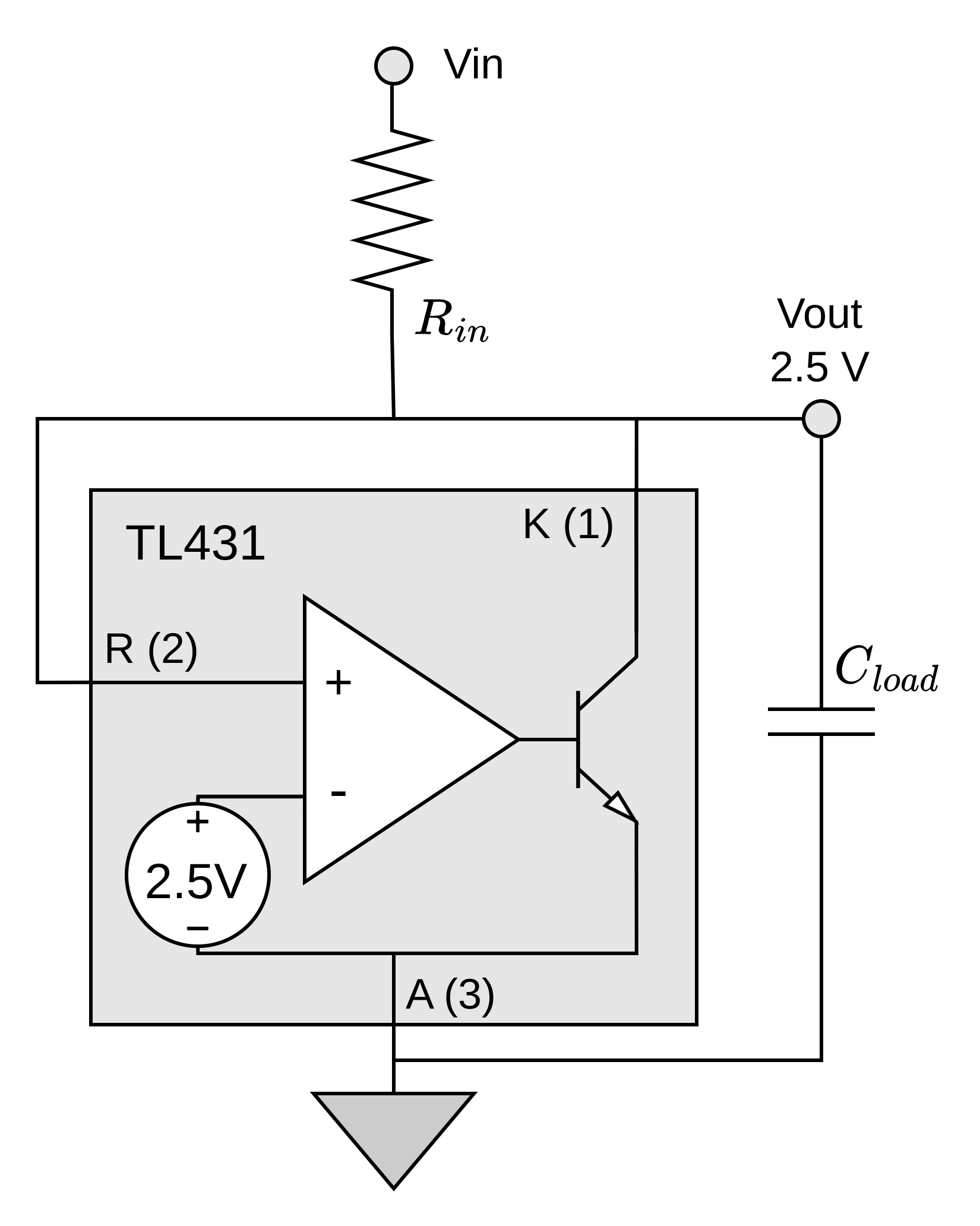
In applications with closed loop regulation the TL431 sinks current through the cathode pin to maintain the voltage on the reference terminal at \(2.5~V\). This lab will be analyzing the TL431 as a shunt voltage regulator and the impact of an output capacitor, \(C_{load}\). The schematic of this configuration is shown in Figure 4.7. In this configuration the cathode and reference pins are connected together and to the positive supply rail through \(R_{in}\) and regulated at \(2.5~V\). A voltage divider can be added between the cathode and reference pin to generate an output voltage greater than \(2.5~V\).
Shunt regulators have some downsides: they consume power at no load and the maximum output current is limited by the supply voltage and \(R_{in}\). However, the circuit is simple and low cost, has good noise rejection, and achieves high DC accuracy with the TL431 (2% - 0.5%). There is one often overlooked design constraint with the shunt regulator: the regulation loop is sensitive to capacitance on the output and some capacitance values may cause the output to oscillate. Given designers propensity for sprinkling capacitors everywhere and the widespread use of the TL431 this is a surprisingly common issue. The lab author has seen this exact issue causing problems in a prototype at a to-be-unnamed major tech company.
You are going to be developing a frequency domain model of the TL431, using it to determine the impact of load capacitance and what values can cause oscillation, and then verifying your results. Although this is a linear regulator, as you will see in lab 3 with the flyback test board, switch-mode power supplies have similar stability issues that are modeled with the same approach and have the same stability concerns.
4.4.1 System Transfer Function
The stability of the system with closed loop feedback can be determined through the phase margin (PM) of the open loop transfer function. Phase margin represents the additional phase shift at the that would be required for the system to oscillate at the crossover frequency when gain is \(1\). The phase shift required for oscillation is \(180^{\circ}\). In textbooks you will often see the phase margin defined as the phase of the transfer function plus \(180^{\circ}\) \((\text{PM} = \phi+180^{\circ})\), but this is for systems where the feedback is abstracted as a subtraction block that is independent of the transfer function. For our system the subtraction of the feedback signal from the reference is occurring inside the TL431 and captured in the open loop gain measurement, so the phase margin is the phase of the open loop gain transfer function.
Phase margin is a way of looking at the stability of the system, both in response to perturbations and to changes in operating conditions. If the phase margin is zero or negative the system will oscillate under closed loop feedback. As most systems are somewhat non-linear, a system with a phase margin a bit above \(0^{\circ}\) may also oscillate. A low phase margin also implies an under-damped response of the closed loop system to a transient. In the context of power supply feedback loop design, a phase margin of at least \(45^{\circ}\) is typically desired.
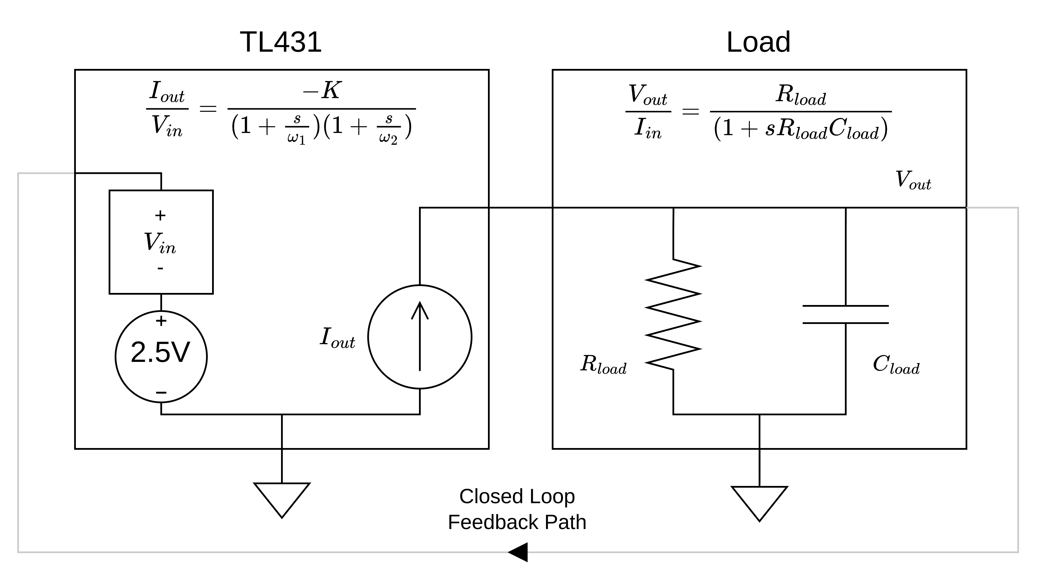
The transfer function for the TL431 shunt regulator system consists of the TL431 itself, which converts an error voltage into an output current, and the load, which converts the TL431 output current into a voltage. This output voltage is then fed back to the reference pin of the TL431 as feedback. From a small signal perspective \(R_{in}\) and \(C_{load}\) are electrically in parallel and comprise the load impedance. The small signal system and the transfer functions of these two elements are shown in Figure 4.8. The open loop transfer function of the system is the product of the TL431 transfer function and the load impedance transfer function. The transfer functions are provided below:
\[\text{TL431: } \frac{I_{out}}{V_{in}} = \frac{-K}{(1+\frac{s}{\omega_1})(1+\frac{s}{\omega_2})}\] \[\text{Load: } \frac{V_{out}}{I_{in}} = \frac{R_{in}}{(1+sR_{in}C_{load})}\] \[\text{System: } \frac{V_{out}}{V_{in}} = \frac{-K R_{in} }{(1+\frac{s}{\omega_1})(1+\frac{s}{\omega_2}) (1+sR_{in}C_{load})}\]
In order to model the system and compute the phase margin for different load capacitors you will be measuring the TL431 open loop gain and extracting the gain, \(K\), and the frequencies of the two poles, \(\omega_1\) and \(\omega_2\).
The presented transfer function of the TL431 may seem arbitrarily chosen, but the two pole system reflects how most internally compensated op-amps are designed, and the TL431 is an oddly connected op-amp. With “dominant pole compensation” a single low frequency pole (\(\omega_1\)) is intentionally added to have the crossover frequency occur before any high frequency parasitic poles due to the circuitry of the op-amp (\(\omega_2\)) that would unacceptably reduce the phase margin. There will be additional poles at even higher frequencies, but just modeling the first is typically accurate enough. For more information on op-amp compensation read the paper Internal and External Op-Amp Compensation: A Control-Centric Tutorial.
4.4.2 Circuits
For this lab you are going to be constructing two copper tape circuits. One circuit, shown in Figure 4.9, will be used to measure the open loop gain of the TL431. The open loop gain of devices with high DC gain can be difficult to measure because any input offset voltage can saturate the output and lead to inaccurate measurements. Typically some sort of low frequency feedback is used to stabilize the system at DC. The circuit you will be using to measure the open loop gain uses \(R_3\) to provide feedback at DC and the feedback is low-pass filtered by \(C_1\). Given the expected low frequency gain of the TL431, the component values will allow for accurate measurement of the open loop gain of the TL431 down to a frequency of \(\approx 500 ~\text{Hz}\), which is signifigantly below \(\omega_1\) and \(\omega_2\).
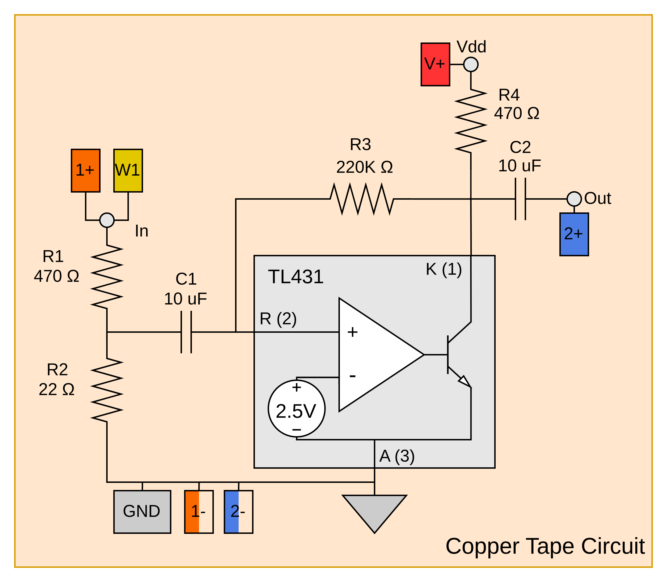
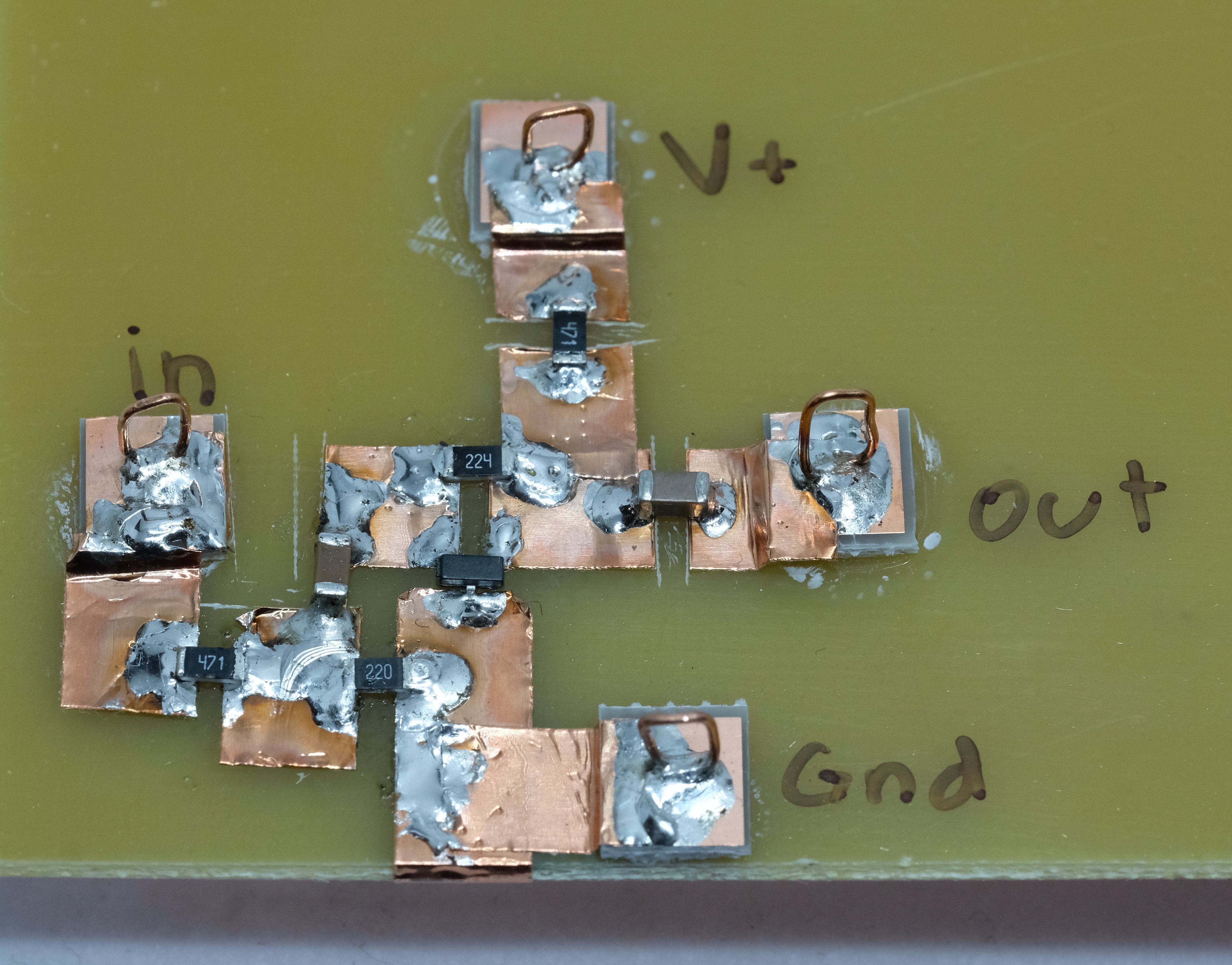
The second circuit is the basic TL431 voltage regulator, shown previously in Figure 4.7, where you will be verifying the (in)stability of the TL431 shunt regulator due to the load capacitor. In constructing the TL431 voltage regulator circuit use a value of \(470\Omega\) for \(R_{in}\). For both circuits use a supply voltage of \(5~V\). This can be supplied from a lab power supply or the internal power supply on the AD2. Figure 4.10 shows a photo of the completed circuit for layout inspiration.
This is mostly relevant to people running the labs in the future. The TL431 comes in two pinouts. If the circuits are not working make sure that the datasheet pinout matches what is shown in the figures.
4.4.3 Measurements
You will use the AD2 and the “Network” menu of the WaveForms software to measure the open loop gain of the TL431 and then export the data for processing by a python script that will fit the data to the two pole transfer function. Network analysis in the WaveForms software is similar to the impedance analysis. A frequency sweep is applied to the input of a system with the function generator and the AD2 measures the input and output amplitude and phase.
Figure 4.11 shows the Network view in WaveForms along with the correct settings to use and a completed sweep of the TL431. C2 (in blue) represents the transfer function of the system normalized to C1, which measures the input amplitude. The top plot shows gain in dB and the bottom plot shows phase in degrees. To collect enough data to accurately extract the DC gain and frequencies of the two poles, sweep from 500 Hz to 5 MHz. Set the amplitude to 10 mV to avoid saturating the TL431 at low frequencies where gain is high. If you do not manually adjust the displayed magnitude range your measurements may extend beyond the Y axis. There can be variation in the the open loop gain and frequencies of the poles between parts, but your measurements should appear broadly similar.
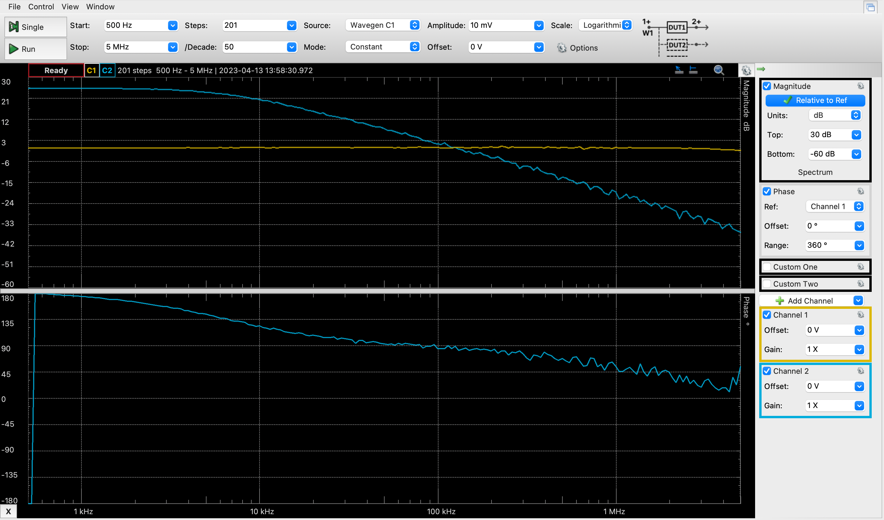
Once the sweep is complete click File>Export on the top left of the screen and export the data. Do not change any of the export options and save the data as TL431_open_loop.csv in the same folder as the python scripts to match the expected naming and location. The python script tf_fit.py is used to extract \(K\), \(\omega_1\) and \(\omega_2\), from the measured data and normalizes the data to account for the \(V/I\) conversion of the load resistor and the attenuation of the input voltage divider. At the top of the script the name of the input data file and output plot image are defined along with the load resistor and input voltage divider. You should not need to change any of these values. When run, the script will print the best fit values for \(K\), \(\omega_1\) and \(\omega_2\) and display and save a plot of the measured data overlaid with the best fit transfer function. If the script was successful the two lines should closely overlap.
The second python script system_tf.py requires the values of \(K\), \(\omega_1\) and \(\omega_2\), extracted by the first script. Replace the placeholder values at the top of the script with the values you extracted. You will be changing the value of load capacitance defined at the top of the script and seeing how that impacts the phase margin. This script models the open loop transfer function of the TL431 and load and generates and saves a plot of the open loop transfer function with the crossover frequency marked and the phase margin calculated. Figure 4.12 shows an example output.
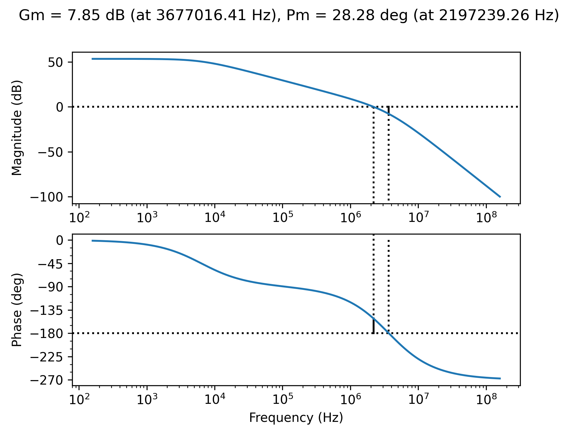
Try iterating through capacitor values in the range of \(10~\mu F\) to \(10~pF\) and see how it impacts the phase margin and crossover frequency. Changing the load capacitor changes the frequency of the output load pole, which is at a frequency of \(\omega = \frac{1}{R_{load}C_{load}}\). A pole is required to roll off gain and achieve a finite crossover frequency, but two poles before crossover causes a \(-180^{\circ}\) phase shift and a low or zero phase margin. In the context of the TL431 voltage regulator this constrains the frequency of the pole due to the output capacitor. The frequency of the output load pole can either be much lower than the low frequency pole of the TL431, \(\omega_1\), such that crossover occurs before \(\omega_1\), or the output load pole can be at a significantly higher frequency than \(\omega_1\) such that it occurs after crossover. You should observe a “danger zone” of capacitance values that lead to a poor phase margin and possible oscillation.
For the lab submission you will need to find a capacitor value which causes the TL431 to oscillate and verify with the oscilloscope. As the phase shift due to a pole only asymptotically approaches \(-90^{\circ}\) you will not be able to reach a phase margin of \(0^{\circ}\) with only two poles. However, due to non-linearity, the system is likely to oscillate if the phase margin is small. You can verify and record the oscillation with either the oscilloscope functionality of the AD2 or one of the lab oscilloscopes.
4.4.4 Tasks
- Provide the plot of the measured TL431 and best fit modeled TL431 gain. What are your extracted values of \(K\), \(\omega_1\) and \(\omega_2\)?
- Using your model of the system find a capacitor value that causes the TL431 output to oscillate. What is the value of the capacitor? What is the modeled phase margin with this capacitor?
- Capture an oscilloscope waveform of the TL431 shunt regulator oscillating with a capacitive load. What is the frequency of oscillation? How does it compare to the modeled crossover frequency and why may it differ?
- Provide a picture of your copper tape circuits.
- (Post Lab) If you added a voltage divider between the cathode and reference pin of the TL431 to regulate at an output voltage greater than \(2.5~V\) how would this impact the crossover frequency of the open loop transfer function?
4.5 Feedback
Please provide feedback to help make future labs better! Anonymous feedback can be provided via this google form. Feedback is strongly appreciated but feel free to skip answering any of these questions.
- Approximately how many hours did this lab take?
- Is there anything that you think should be removed from the lab? If so, what?
- Is there anything that you wish the lab included or elaborated more on? If so, what?
- What is the most useful thing that you learned from this lab?