4 Experimental Procedure
Required Tools:
- Flyback Test Board
- Oscilloscope with two 10x voltage probes
- DC Power Supply
- DC Load
- Soldering Iron
This lab requires soldering the resistor-capacitor snubber network on the board. The resistor is package size 1206 and the capacitor is package size 0805. SMD component kits of each should be in the lab.
4.1 Board Setup
Acquire a test board from the pile on the table. Write the names of you and your lab partner on a piece of masking tape and stick it to the back side of the PCB. You will be making modifications to the board over the course of the class, so it is important you track which is yours. The board can be left on the shelf in lab or you may take it with you.
The power and load connections to the test board are made with 3.5mm pluggable terminal blocks. There is a bag of the terminal blocks on the counter. Some of the lab power supplies and loads may already have cables with terminal blocks attached. If not it is suggested you use the spool of zip cord (red and black two conductor cable) to connect the terminal blocks to the power supply and load.
For this lab you will not be using the load built in to the test board or working with the control loop. Make sure both switches for the on-board load are set to “Off” (down) and the feedback select pin is set to “Direct” (down).
For all of the parts of this lab set the DC power supply to current limit of \(1~A\). If you set the current limit too low the power supply may power cycle when you load the flyback converter, if you set the current limit too high it increases the risk you damage the board if you accidentally short something out.
4.2 Converter Efficiency
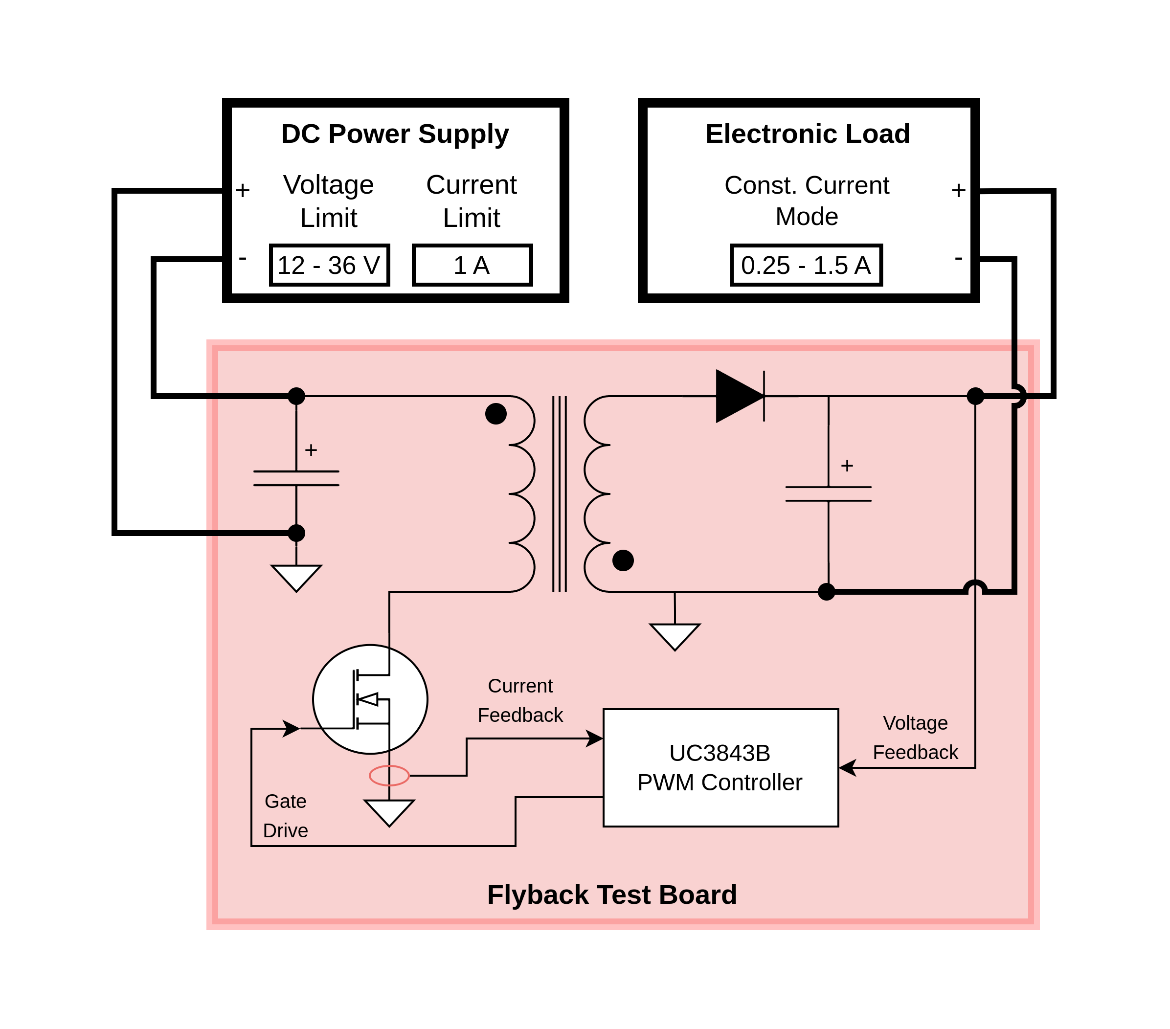
One of the most important metrics of a power supply is the efficiency. For this part of the lab you will be measuring the efficiency of the flyback converter across load and input voltage. You will be using the electric load in constant current mode connected to the output of the flyback converter to provide a load and to measure the output power. The input power to the test board can be measured via the metering on the lab power supply, or you may use external DMMs for greater accuracy. (Figure 4.1) shows a diagram of the test setup for measuring efficiency. You will also be using this test setup with the DC load to conduct the other portions of the lab.
4.2.1 Tasks
- Measure the efficiency of the flyback converter over a load range of \(0.25~A\) - \(1.5~A\) in \(0.25~A\) increments and input voltages of \(12~V\), \(24~V\) and \(32~V\).
- Create a plot overlaying the efficiency curves over load current for the three input voltages.
- (Post Lab) List 3 components where power is dissipated in the flyback converter, provide the component reference designators of those components from the schematic.
4.3 Snubber Design
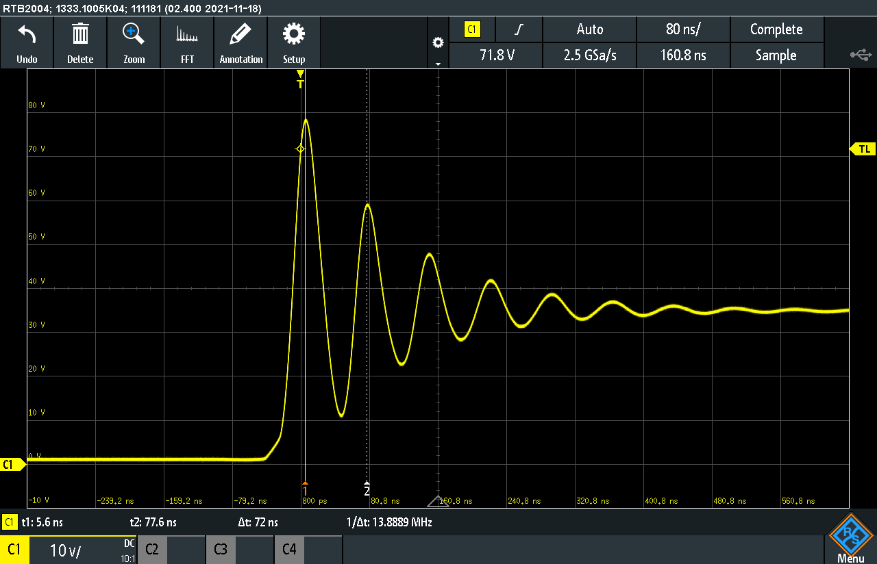
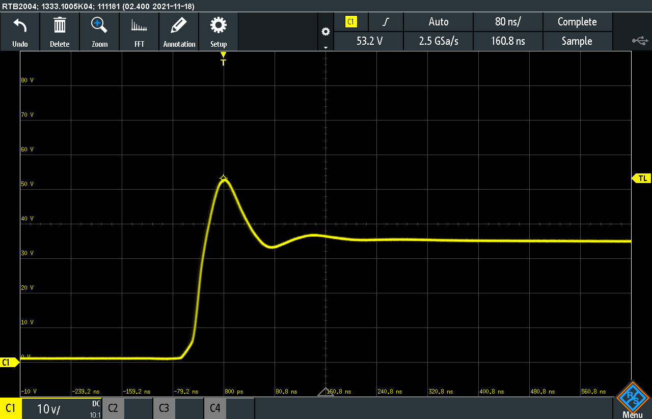
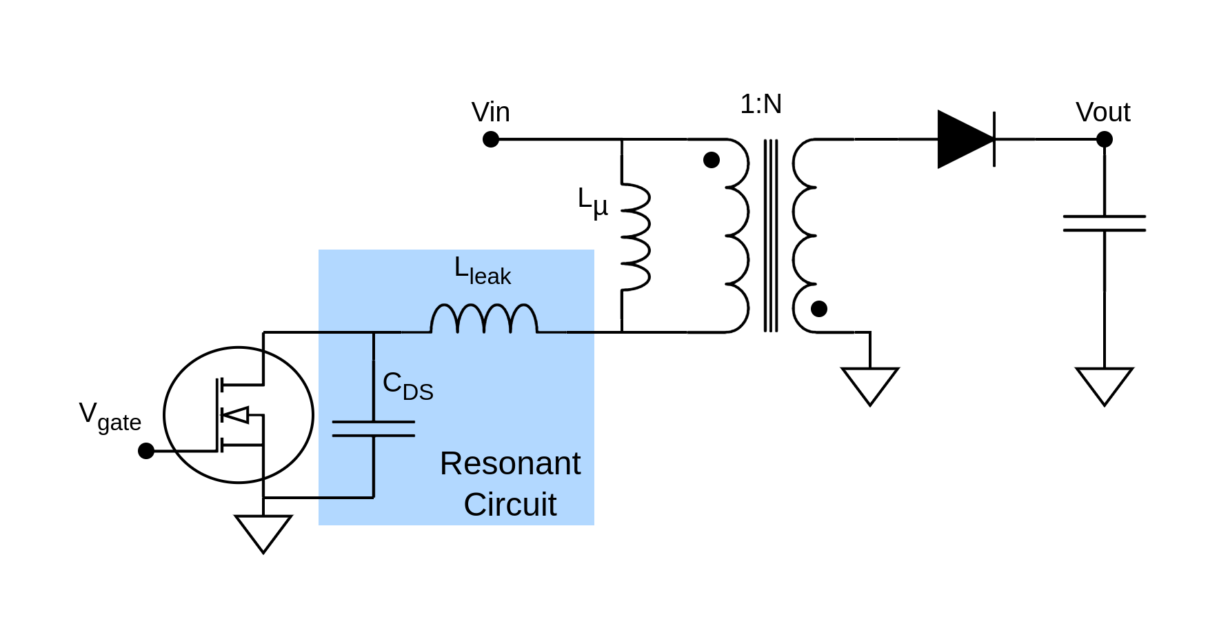
Switch-mode power supplies are one of the largest offenders in emitting EMI (electromagnetic interference), which can interfere with other devices and radio communication. There are strict regulations on the EMI emissions from all electronic products and addressing EMI is a crucial task in the design of any switch-mode power supply. In the flyback converter the ringing, or oscillation, of the MOSFET drain to source voltage, \(V_{DS}\), on turn-off can be a significant source of EMI. This ringing will also interfere with some of the measurements you need to take on the flyback test board. In this part of the lab you will characterize the source of the ringing and add a RC (resistor-capacitor) snubber to dampen it so that it will not interfere with any future measurements you make. Figure 4.2 shows \(V_{DS}\) at turn off before and after the addition of a RC snubber network.
The cause of ringing in switching waveforms is typically due to parasitic, or unwanted, circuit elements. In the flyback converter the ringing on turn-off is between the drain to source capacitance of the MOSFET, \(C_{DS}\), and the leakage inductance of the transformer, \(L_{leak}\). When the power MOSFET in the flyback converter is on, energy is transferred to the magnetizing inductance of the transformer, \(L_\mu\). When the MOSFET turns off, the energy in the transformer commutates the rectifier diode and delivers power to the output. However, the energy stored in the \(L_{leak}\) is not coupled to the output and oscillates with \(C_{DS}\). Figure 4.3 shows the flyback converter with these parasitic components shown as well as the small signal model with the RC snubber added. As the MOSFET is off and the diode is an AC short across the transformer secondary both the MOSFET symbol and the transformer are removed from the small signal model and do not impact the oscillation.
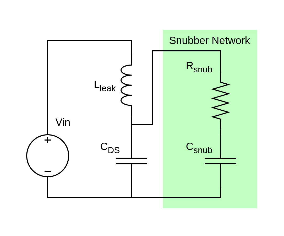
Without the RC snubber, the frequency of the ringing is determined solely by \(L_{leak}\) and \(C_{DS}\). The initial conditions and amplitude of this resonance are set by the current though \(L_{leak}\) at turn off. The resonance is only lightly damped by the inherent losses in \(L_{leak}\) and \(C_{DS}\), so the oscillations can continue for many cycles, decaying exponentially until \(V_{DS}\) is at the expected steady state voltage for the flyback converter.
The design approach that you will be using for the RC snubber is to make \(C_{snub} \gg C_{DS}\) such that the circuit can be approximated as a series RLC circuit and then choosing the value of \(R_{snub}\) to damp the resonance. Below are two equations to help you in the design, the resonant frequency, \(f\), of a LC circuit, and the damping factor, \(\zeta\) for a series RLC circuit. A lower damping factor represents oscillations that dampen more quickly. You will be targeting \(\zeta = 1.0\) for your snubber design, which is considered “critically damped” where the circuit settles to the steady state value as quickly as possible without oscillations.
\[ f = \frac{1}{2 \pi \sqrt{ L C}} \] \[ \zeta = \frac{R}{2}\sqrt{\frac{C}{L}} \]
For the design of the snubber you will first measure the values of \(C_{DS}\) and \(L_{leak}\) in circuit by measuring the resonant frequency. \(C_{DS}\) and \(L_{leak}\) can technically be obtained from the datasheets of the MOSFET and transformer, but other components and the PCB layout itself can add capacitance and inductance, so its more accurate to measure in-circuit. Once you have these values you will be able to calculate values for the RC snubber, install the components, and measure the final waveforms.
R21 (\(R_{snub}\)) and C11 (\(C_{snub}\)) are relatively large SMD components connected to a copper pour that conducts away heat. These will be the most difficult components to solder and de-solder for all of the labs.
When de-soldering make sure there is enough solder on the iron such that it can make good contact and transfer heat to the pads. Try using two irons at once, one to heat up both sides of the component.
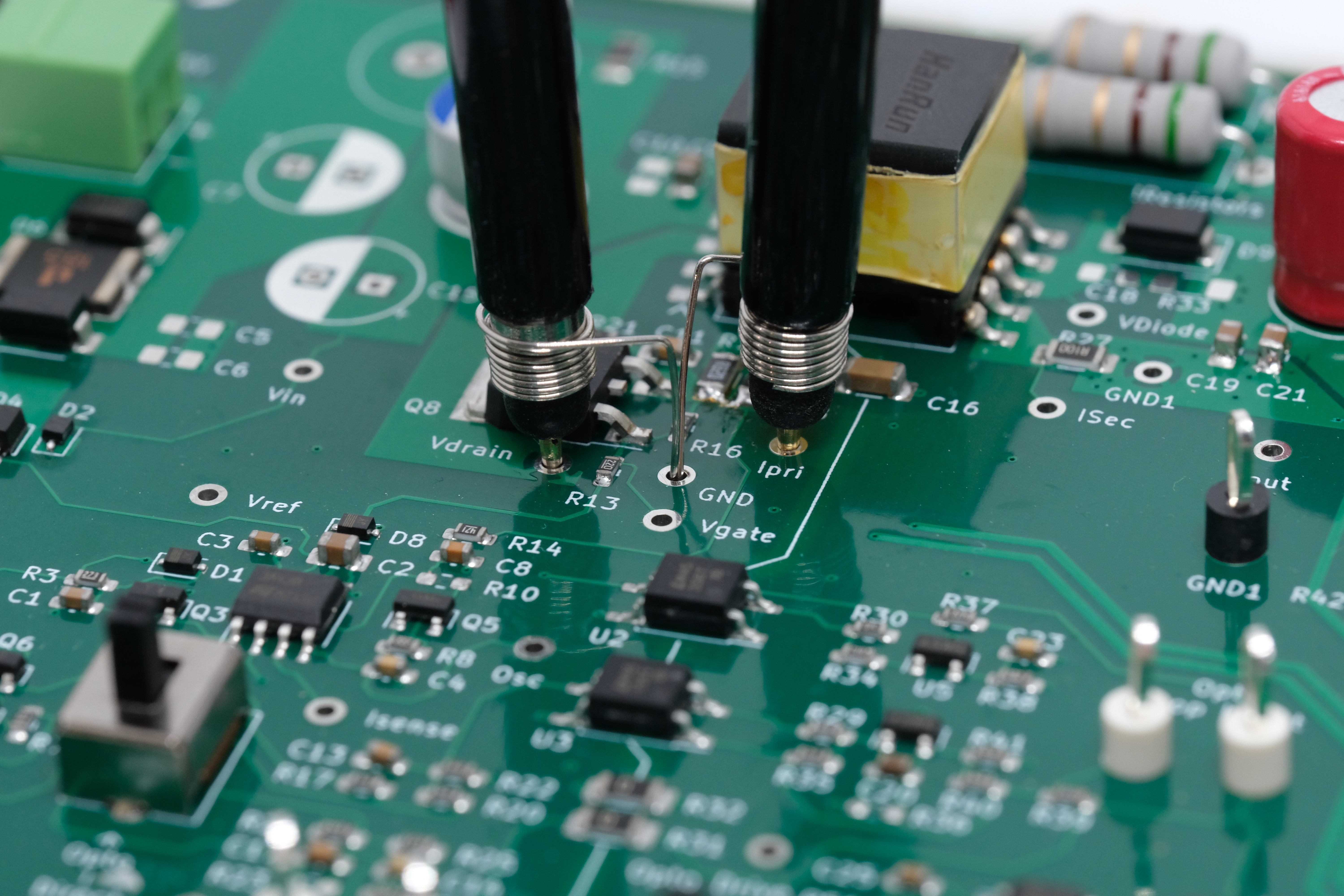
As switching transitions occur very fast the inductance of the oscilloscope ground leads can cause signal integrity issues. For measurements of the switching waveforms we recommend you use the ground spring for the oscilloscope probe. There should be enough space to directly seat the oscilloscope probe tip in the test point holes and have the ground spring of each oscilloscope probe directly in the hole of the adjacent “GND” test point. (Figure 4.4) shows the ideal probe connections.
4.3.1 Tasks
All measurements to be taken at an input voltage of \(24~V\) and an output load of \(1~A\).
- With \(C_{snub}\) (C11) and \(R_{snub}\) (R21) not installed measure the frequency of the ringing on \(V_{DS}\) during turn-off, \(f_1\). Use the oscilloscope cursors to help you measure the ringing frequency. Save an oscilloscope screenshot for your lab submission.
- Solder in a \(100~pF\) capacitor for \(C_{snub}\) and a zero ohm resistor or wire short for \(R_{snub}\). Measure the frequency during turn off, \(f_2\).
- Given the measured frequencies, \(f_1\) and \(f_2\), and the known additional capacitance in parallel with \(C_{DS}\) when measuring \(f_2\), calculate the values of \(L_{leak}\) and \(C_{DS}\).
- Choose \(C_{snub}\) to be three to five times greater than the value you calculated for \(C_{DS}\), subject to the values available in the SMD capacitor kit. This is satisfactory to assume \(C_{snub} \gg C_{DS}\). Calculate \(R_{snub}\) such that \(\zeta = 1.0\) and choose the closest value of resistor available in the SMD capacitor kit.
- Solder in the new components for \(C_{snub}\) and \(R_{snub}\). Measure and save an oscilloscope screenshot of the new turn-off transition for your lab submission.
4.4 Measuring Switching Loss
The power MOSFET is not an ideal switch. The device has an on-resistance which causes a power dissipation of \(I^2R_{on}\) when conducting current. When the device is off the current flow is small enough such that losses can typically be considered negligible. The on resistance is an important parameter in calculating the loss in the power MOSFET, and in EE153/253 you measured the on-resistance of devices and used those values to calculate loss. However, there is another loss that is significant in power electronics applications: Switching Loss.
Switching loss is the power dissipated when the MOSFET takes a finite amount of time to transition from the on and off states. Although the device can transition quite fast (in the nanosecond range) the voltage and current are both high so the peak power dissipated is large. In a switch-mode power supply where the MOSFET is switching thousands of times a second this can lead to significant power dissipation. Figure 4.5 shows how the overlapping transitions in voltage and current cause power dissipation.
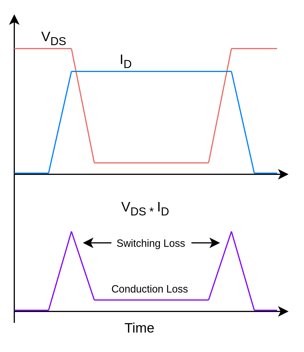
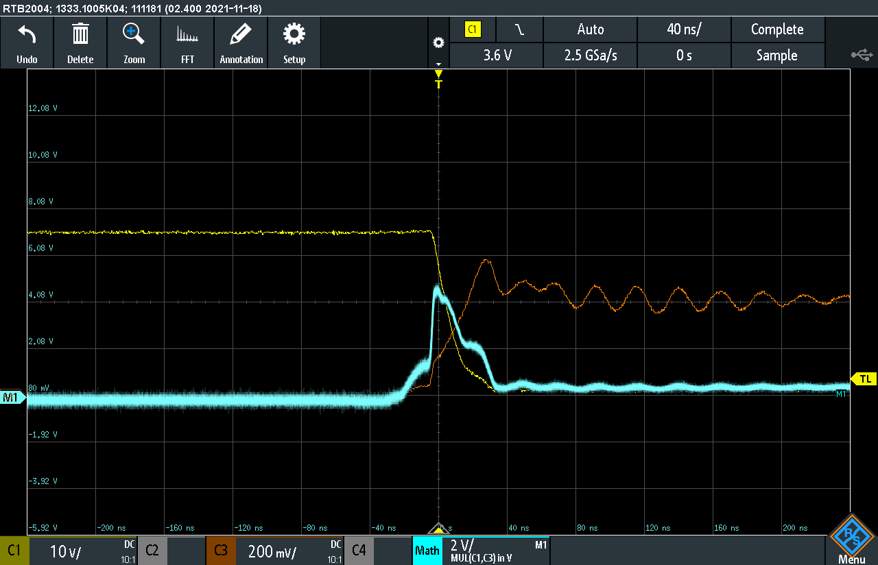
In this portion of the lab you will measure switching loss when the power MOSFET in the flyback converter turns on and off. This can be done by using the oscilloscope to measure the MOSFET drain to source voltage, \(V_{DS}\), and drain current, \(I_D\), during the switching transitions. \(V_{DS}\) can be measured at the “Vdrain” test point on the test board while \(I_D\) can be measured at the “Ipri” test point, which connects to two parallel \(0.75~\Omega\) resistors between the MOSFET source and ground. These shunt resistors are used by the controller IC to regulate the MOSFET current but for this test setup it can be used to measure the MOSFET current without a dedicated current probe.
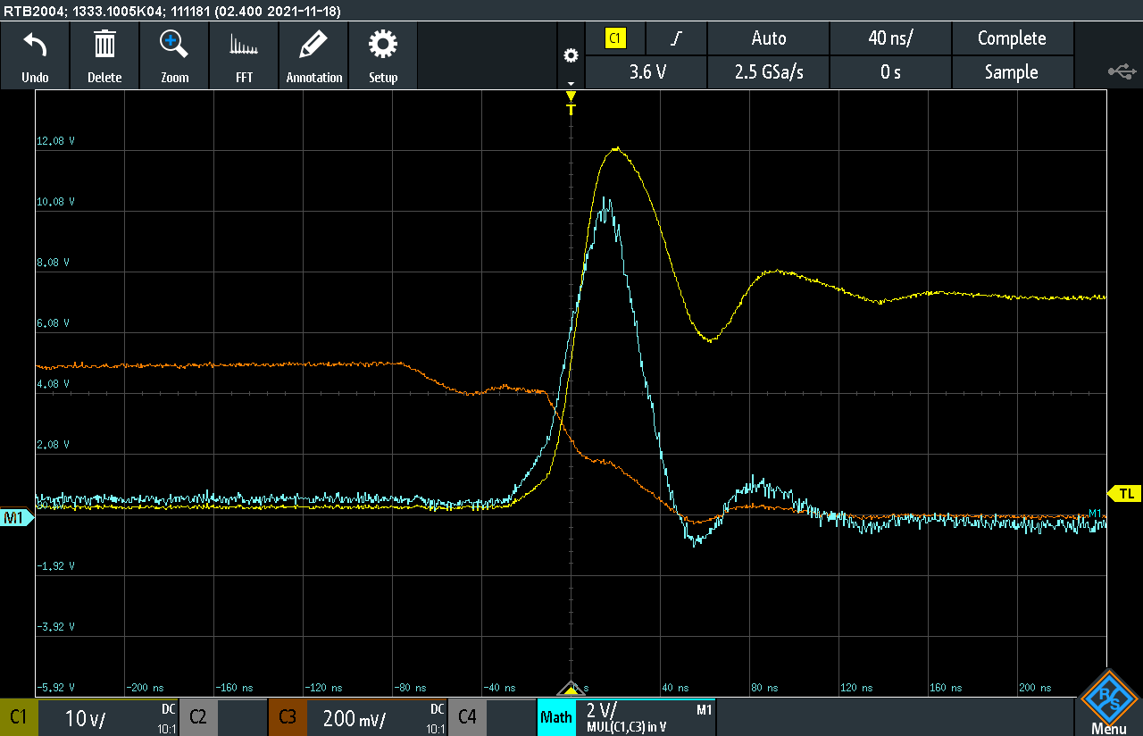
The energy dissipated during each switching transitions is the integral of \(V_{DS} \cdot V_{D}\). For this lab you can approximate the \(V_{DS} \cdot V_{D}\) waveform during the switching transitions as a triangle. Use the “Math” function on the oscilloscope to display \(V_{DS} \cdot V_{D}\) and use the oscilloscope cursors to read off your best estimate of the width and height to approximate the area. Make sure to scale your result by the 0.375V/A sensitivity of the current sense resistors. (Figure 4.6) shows example waveforms of the turn-on and turn-off switching transitions with the math trace showing \(V_{DS} \cdot V_{D}\).
4.4.1 Tasks
All measurements to be taken at an input voltage of \(24~V\) and an output load of \(1~A\).
- Provide oscilloscope screenshots of the turn-on and turn-off switching transitions.
- Calculate the turn-on and turn-off switching loss. Your answer should be in units of Joules.
- (Post Lab) The flyback converter switches at approximately \(250~kHz\). Calculate the time averaged switching loss in watts. Using your results from measuring the converter efficiency, what percentage of the total power loss is switching loss?
- (Post Lab) As the MOSFET switches faster switching loss is reduced. The MOSFET gate can be modeled as a capacitor and the transition time is dependent on the resistance of the driving source. What is the reference designator of the resistor in the schematic which could be reduced in value to reduce the duration of the switching transition?
4.4.2 Feedback
Please provide feedback to help make future labs better! Anonymous feedback can be provided via this google form. Feedback is strongly appreciated but feel free to skip answering any of these questions.
- Approximately how many hours did this lab take?
- Is there anything that you think should be removed from the lab? If so, what?
- Is there anything that you wish the lab included or elaborated more on? If so, what?
- What is the most useful thing that you learned from this lab?