1 Introduction
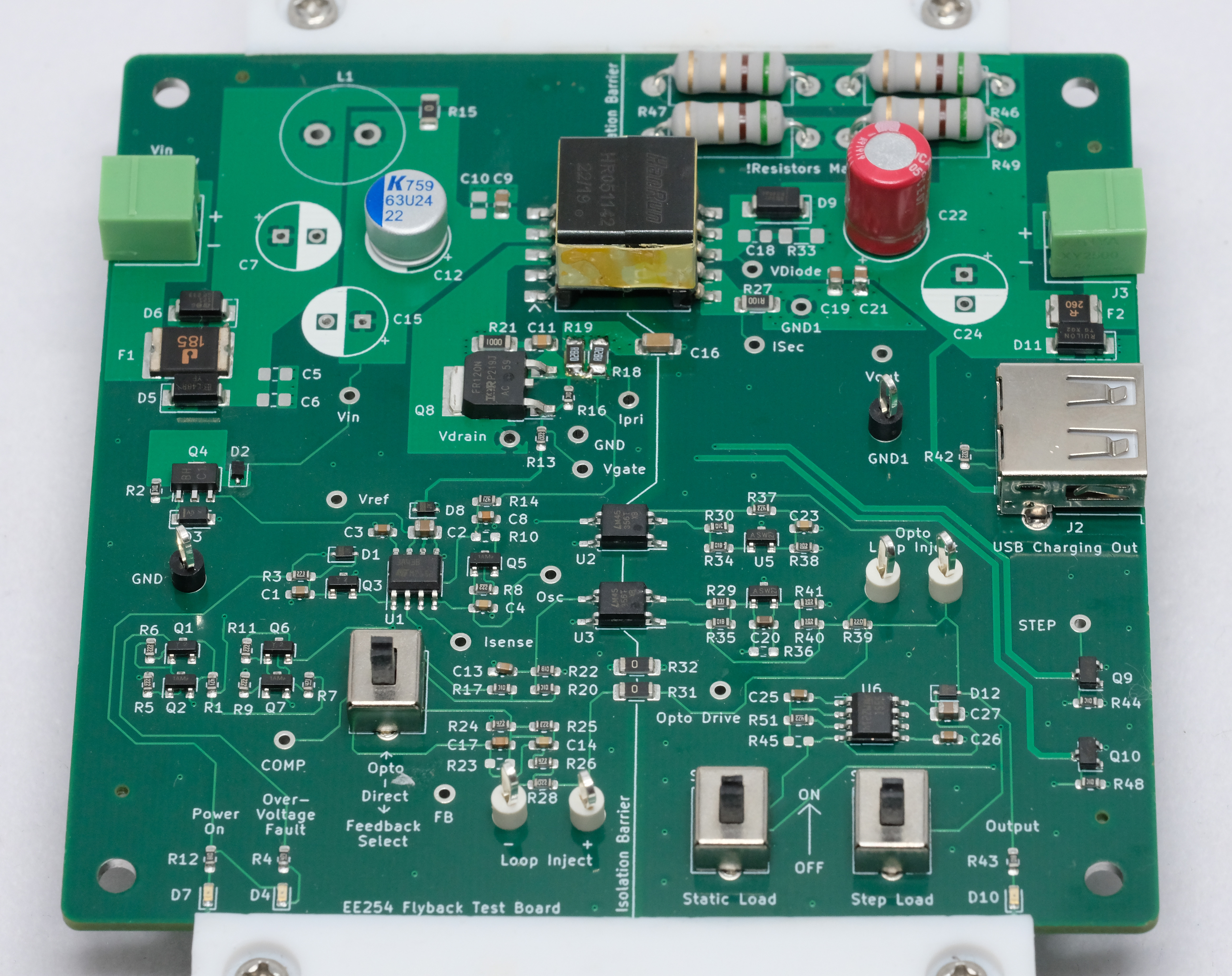
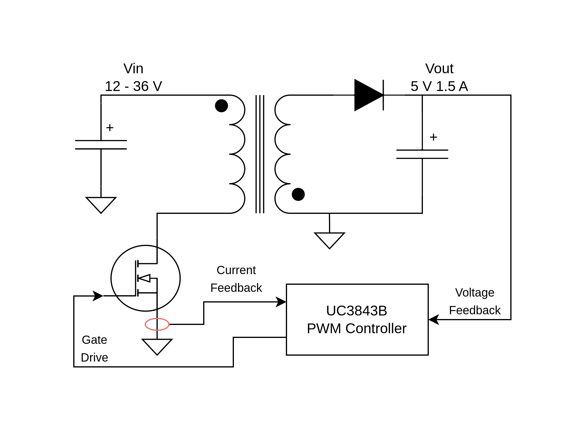
The labs for this class are based on the EE254 flyback test board, shown in Figure 1.1. The board accepts a 12-36V DC input and provides a regulated 5V output which capable of charging a phone through the USB-A connector. As a flyback converter this board is similar to the flyback converter you built in EE153/253. Figure 1.2 shows a simplified diagram of the test board. Compared to the flyback converter you built in EE153/253, this board has a control loop to regulate the output voltage as well as added test points, protection circuity, and a small DC load, to make work with the board easier.
Over the course of the labs you will be characterizing the performance of the flyback converter and improving the switching waveforms and response of the control loop that regulates the output voltage. Hopefully you will feel confident enough in the board by the end of the class to try using it to charge your own cell phone! The goal of this first lab is to familiarize you with the operation of the test board and comfortable taking measurements with some of the lab equipment.
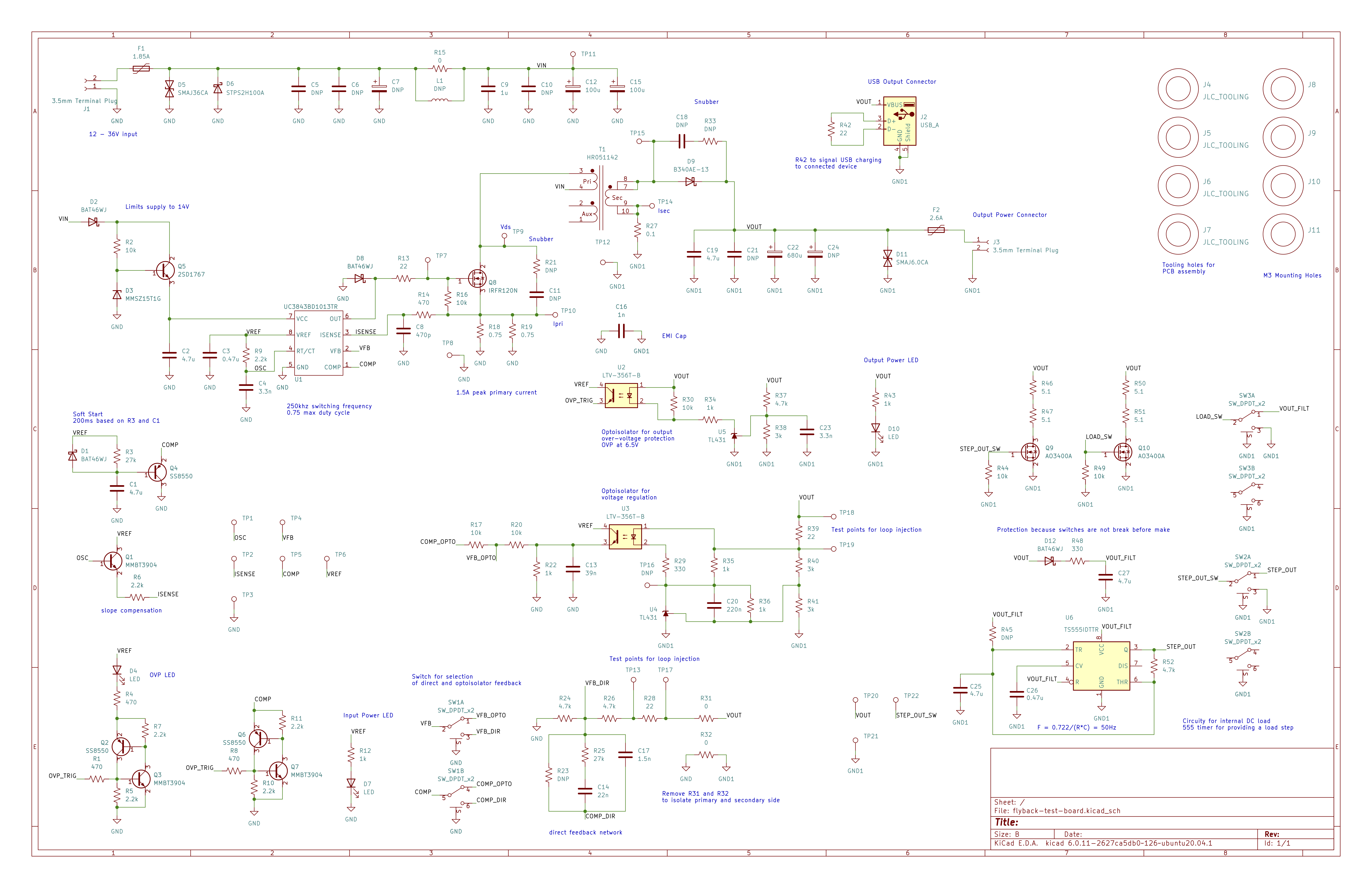
The flyback test board was designed in kicad. The github repo containing the kicad design files and an annotated PDF schematic is here. The components on the test board are well labeled and the PDF schematic should be sufficient for the labs but it is highly recommended you try downloading kicad and looking at the PCB layout. The schematic is also provided in (Figure 1.3).
In this lab you will be conducting some common first tasks for evaluation and bring-up of new power supply design:
- Measuring efficiency
- Measuring switching waveforms
- Improving switching waveforms